Construction of a 1D flexible topological VCSEL by use of synthetic parameter space
In condensed matter physics, the combination of the time-reversal and space-inversion symmetries protects the gapless properties of Dirac fermions in graphene. However, by introducing atoms with different masses in the honeycomb lattice and breaking the inversion symmetry, an energy gap can be created while there is no topological edge state within the bandgap. This system, insulating both in the bulk and along its edge, is called a Semenov insulator, as first discussed by Semenov44,45. Although Semenov insulators, such as boron nitride (BN) and silicon carbide (SiC) lattice structures, exhibit topologically trivial properties, it is well established that juxtaposing two “mass-inversed” BN lattices with different valley Chern numbers can lead to a topologically protected mode, in a manner similar to the quantum valley Hall effect46,47,48,49,50.
According to the Hamiltonian described by the Dirac equation, it can be found that the on-site potential can be equivalent to the mass term of the atom within a unit cell51. Recently, Huang et al. designed an acoustic structure based on the discrete spring mass model and modulated the height of the resonator to simulate the disturbed mass52. The calculated band structure shows that one interface state can also be generated by juxtaposing two topologically trivial structures with inversion symmetry broken, and the sound wave can be strongly localized at the interface. The similarities between this 1D system and a 2D hexagonal BN lattice make us wonder whether a 1D equally-coupled and site-potential modulated diatomic chain can have similar topological properties with the 2D quantum valley Hall effect.
In general, the dimension of a physical system is determined by its geometry. Constructing a synthetic space by coupling states in an artificial lattice or introducing structural parameters can provide an ingenious way to realize a high-dimensional system53,54,55. Here, we construct a 1D flexible metastructural superlattice with PCLC films and polymer Mylar films. By adjusting the thickness of the Mylar films, the on-site potentials are modulated, similar to the mass modulation in Semenov insulators.
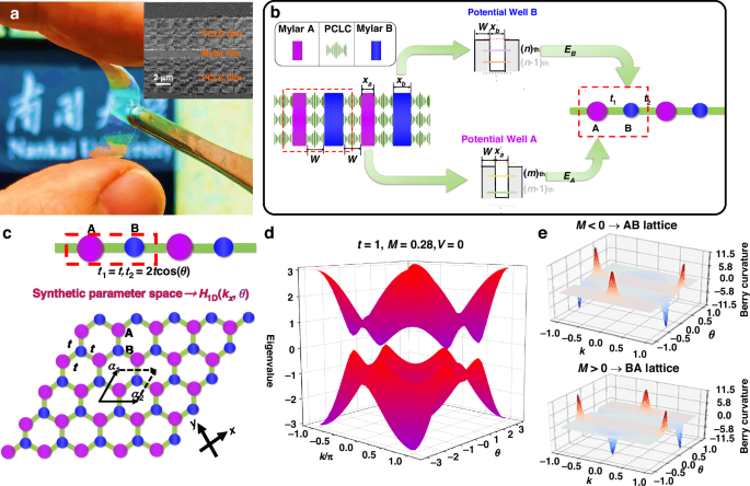
Based on the optical quantum-well theory, we first analyze the 1D optical potential well composed of an isotropic polymer layer (transparent film) inserted between two free-standing PCLC layers (selective reflection films), as shown in Fig. 1a. The multilayer films were cut and sprayed with gold powder so as to observe their cross-sectional SEM image, as illustrated in the upright inset. Studies have shown that one or more defect modes can be introduced into the polarization band gap of the CLC by adding isotropic layers and/or pitch jumps within the CLC helix56. Here, the PCLC has the characteristics as 1D photonic crystals, and its polarization band gap limits the propagation of light at specific frequencies and polarizations, so it can be regarded as an optical potential barrier. A commercially available isotropic Mylar film (Mylar D, DuPont) is inserted into the PCLC, which serves as a potential well to form an optical quantum well57,58. The width of the single potential well is so narrow that the motion of the photons along the direction perpendicular to the well walls exhibits quantized characteristics, and the energies take discrete values in the polarization band gap of the PCLC. Similar to the semiconductor quantum wells, the frequencies of the photon bound states decrease as the well width increases59,60,61. [see Supplementary Note 1 of SI].
a Photography of a free-standing three-layer metastructure consisting of an isotropic Mylar layer (transparent film) sandwiched between two free-standing PCLC layers (selective reflection films). The upper right inset shows the cross-sectional scanning electron microscope (SEM) image of this free-standing structure. b Schematic diagram of a 1D AB diatomic chain assembled by two kinds of optical potential wells (Mylar films of different thickness). c Introducing coupling coefficient modulation in the 1D AB diatomic chain to construct a synthetic parameter space in analogy with a 2D Semenov insulator. Here, coupling strength t1 = t, t ∈ R, and t2 is a variable, \({{{t}}}_{2}=2{{t}}\cos \left({{\theta }}\right),{{\theta }}\in \left[-{\rm{\pi }},{\rm{\pi }}\right]\). d Band structure of the coupling-modulated diatomic chain in the k-θ synthetic parameter space. e Berry curvature of the energy bands below the band gap in the synthetic parameter space for the AB- and BA-type diatomic lattices
For the optical lattice shown in Fig. 1b, different thicknesses of Mylar films cause the change of the coupling energy levels in adjacent potential wells, which in turn change the on-site potentials. Here, we consider only the nearest neighbor coupling, that is, one set of energy levels that can be coupled in the adjacent A and B quantum wells, such as the mth energy level in the A potential well and the nth energy level in the B potential well. The corresponding energies are defined as EA and EB, which can also be considered as the on-site potentials of A and B sites according to Fig. 1b.
The 1D diatomic chain consists of N unit cells, and each unit cell hosts two sites (potential wells A and B). Under the tight-binding approximation where only nearest-neighbor interactions are retained, the Hamiltonian of this 1D diatomic chain can be expressed as:
$${{\rm{H}}}_{1{\rm{D}}}=\left[\begin{array}{cc}{{V}}-{{M}} & {{{t}}}_{1}+{{{t}}}_{2}{{\rm{e}}}^{{\rm{i}}{{k}}}\\ {{{t}}}_{1}+{{{t}}}_{2}{{\rm{e}}}^{-{\rm{i}}{{k}}}{} & {{V}}+{{M}}\end{array}\right]$$
(1)
where t1 and t2 represent the coupling term between the nearest neighbor potential wells. V ± M represents the potentials on A and B sites. The V (average potential of A and B sites) is a constant term to the energy. M describes the difference in potentials between A and B sites. Notably, this 1D diatomic chain has spatial inversion symmetry only when the potentials of A and B sites are equal, namely M = 0. As a result, M is often called the inversion symmetry breaking mass, or the Semenov mass62. To explore the topological origin of the 1D onsite-potential modulated diatomic chain, we set t1 = t, t2 = 2t cos(θ), in which θ=[−π, π] and t ∈ R, so that we form a synthetic parameter space. The term 2t cos (θ) can be rewritten as \(2{{t}}\cos \left(\theta \right)={{t}}({e}^{{\rm{i}}\theta }+{e}^{-{\rm{i}}\theta })\), and Eq. (1) transforms into:
$${{\rm{H}}}_{2{\rm{D}}}\left(k,\theta \right)=\left[\begin{array}{cc}V-M & {{t}}+{{t}}({e}^{{\rm{i}}\left({k}_{x}a+{k}_{y}b\right)}+{e}^{{\rm{i}}\left({k}_{x}a-{k}_{y}b\right)})\\ {{t}}+{{t}}({e}^{-{\rm{i}}\left({k}_{x}a+{k}_{y}b\right)}+{e}^{-{\rm{i}}\left({k}_{x}a-{k}_{y}b\right)}) & V+M\end{array}\right]$$
(2)
where some substitutions are used (e.g., \(k=\)kx\(a\) and \(\theta =\)ky\(b\)). \({{\boldsymbol{a}}}_{{\bf{1}}}={{a}}\vec{{{x}}}+{{b}}\vec{{{y}}}\) and \({{\boldsymbol{a}}}_{{\bf{2}}}={{a}}\vec{{{x}}}-{{b}}\vec{{{y}}}\) are the basis vectors in the real space, in which a and b depend on the lattice constants. Here, θ acts as a synthetic parameter, enabling us to map this 1D model onto a 2D inversion-symmetry-breaking Semenov insulator, as illustrated in Fig. 1c. The topological properties of this equally-coupled and on-site-potential-modulated diatomic chain can be understood by analyzing a specific case (ky\({b=}\)π ⁄ 3) of the 2D Semenov insulator. From Eq. (2), the band structure of the 1D onsite-potential and coupling-modulated diatomic chain in the k–θ synthetic parametric space can be calculated as shown in Fig. 1d. A band gap opens at Dirac points, showing typical characteristics of the Semenov insulators.
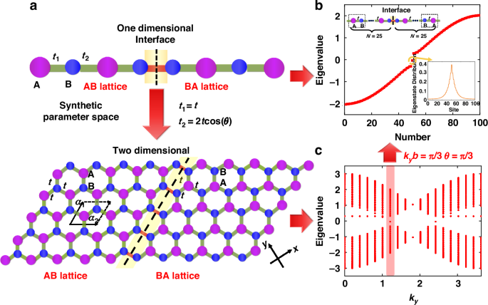
As Fig. 1e shows, the calculated Berry curvature63,64 of the energy bands below the band gap in the synthetic parameter space for the AB lattices has an opposite sign as compared with that for the BA lattices. From M < 0 to M > 0, A and B atoms are exchanged in the lattices. The valley Chern numbers can be computed by integrating the Berry curvature, which are approximately equal to – 0.4 and + 0.4 for AB and BA lattices at K’ point, respectively. Here, the Chern numbers deviate from the ideal value of ± 0.5, possibly due to that the extension of the Berry curvature causes the reduction of the integral for the Chern number46,48. Consequently, AB and BA lattices have different valley Chern numbers, which leads to a topologically protected interface mode as shown in Fig. 2a, analogous to the quantum valley Hall effect65.
a Schematic diagram of the corresponding relationship between the 1D and 2D juxtaposed structures. The yellow areas and dashed lines mark the location of the interface, and both structures on either side of the interface break the inversion symmetry. b Eigenvalues and TIS distribution in the 1D equally-coupled diatomic chain. N represents the number of the unit cells at either side of the interface. A topologically protected edge mode is localized at the interface of the AB and BA lattices. c Dispersion relationship of the 2D structure juxtaposed by AB and BA lattices with different valley Chern numbers. Here, we set t = 1, b = \(\sqrt{3}\)/2 and M = 0.28 in our calculation. The red area marks the special points satisfying kyb = π/3, namely the cross sections θ = π/3 in the synthetic parameter space. In this case, the coupling strength t1 is equal to t2 (t1 = t2 > 0) in the 1D diatomic chain structure
Similar to the discussion in the 2D BN lattice structure and other Semenov insulators, we pay attention to the difference in topological properties caused by the Semenov mass M, so we only consider the case of t1 = t2 > 0 in Fig. 2a. From the dispersion relationship shown in Fig. 2c, we can find the topological interfaces states (TISs) inside the band gap, which are caused by juxtaposing two Semenov insulators with different valley Chern numbers. At the special point kyb = π/3, the eigenvalue of the TIS is located exactly in the center of the band gap. According to the corresponding relationship in Eq. (2), this particular point also corresponds to the cross section θ = π/3 of the synthetic parameter space. Thus, we can construct a simple 1D equally-coupled diatomic chain with only on-site potential modulated. For example, when we place two equally-coupled diatomic chains (AB and BA) side by side, each with 25 unit cells, a TIS appears right in the center of the band gap, localized at the interface as shown in Fig. 2b.
Further, our optical superlattice is a multi-energy level system. Energy levels with the same energy may correspond to different orders in different potential wells, as shown in Supplementary Table S1 of the SI. It can be found that there are a group of Mylar films with different thicknesses corresponding to the same wavelength of 574 nm, that is, potential wells with different widths can have different energy levels corresponding to the same energy. The quantum size effect and multi-level characteristics of quantum wells allow a bandgap closure to occur even when different Mylar films are used as A, B sites, as shown in the Supplementary Note 2 of the SI.
Topological interface states in a soft-matter based VCSEL
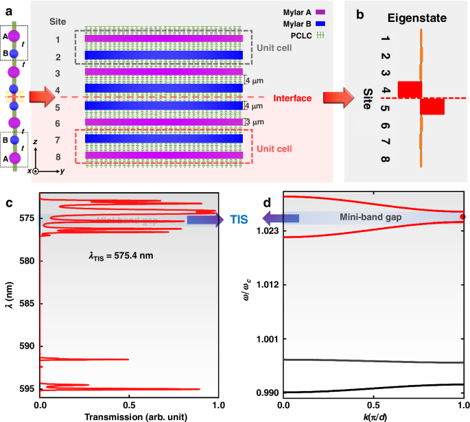
The above illustration and analysis reveal the topological origin of the 1D equally-coupled diatomic chain model with only on-site potential modulated. Next, we provide further theoretical calculation and experimental measurement, and finally achieve a topological VCSEL based on this optical superlattice model. Here, we choose “3 μm” -thick Mylar films (as A sites) and “4 μm” -thick Mylar films (as B sites) to construct AB lattice and BA lattice (Fig. 3a). The on-site potentials in the sub-structures of gray and red areas satisfy EA > EB (M < 0) and EA < EB (M > 0), respectively. The topological phase transition process of the AB and BA equally-coupled diatomic chains can also be verified according to the symmetry of the electric field distributions of the eigenstates above and below their common band gap at the edge of the first Brillouin region, as shown in the Supplementary Note 3 of the SI. Here, potential wells A and B have similar energies near the wavelength of 575 nm, corresponding to the mth and nth energy levels, respectively. Due to the tunneling and coupling between potential wells A and B, the original degenerate energy levels split, and a series of splitting resonance peaks appear in the transmission spectrum59,60,61. In turn, mini-bands are formed and mini-band gaps are generated. This phenomenon can also be analyzed according to the tight binding method66.
a Illustration of the 1D topological VCSEL structure composed of two distinct sub-superlattices with different topological properties, which is equivalent to a 1D equally-coupled diatomic chain with different on-site potentials. b Eigenstate distribution of the TIS. c Transmission spectrum and d mini-band structure of the topological optical superlattice, where the arrows mark the in-gap TIS
By juxtaposing two topologically unequal AB lattice and BA lattice with different valley Chern numbers, a TIS which is highly localized at the interface can be generated, as shown in Fig. 3b. It is clear that this result is in agreement with the theoretical calculation of the 1D equally-coupled diatomic chain model shown in Fig. 2a, b. From the calculated transmission spectrum and the mini-band structure of the superlattice, it can be found that the TIS with the wavelength of 575.4 nm originates from one of the bulk states and evolves into the mini-band gap, that is, one bulk state turns into the TIS, as indicated by the arrows in Fig. 3c, d. In addition, because the energy levels Em−1 and En−1 inside the two potential wells A and B have a large energy difference, light between the nearest potential wells cannot couple. As a result, we cannot find any TIS within 590–598 nm.
In order to experimentally verify the correctness of the theoretical calculation, the metastructural superlattice shown in Fig. 3a was prepared by using Mylar films stacked with PCLC films. The detailed preparation process is described and shown in the next section and Materials and Methods. The transmission spectra of the AB lattice structure and the superlattice after juxtaposition were tested as shown in the Supplementary Note 4 of the SI. A mini-bandgap can be clearly observed in the transmission spectrum of the AB lattice. A TIS with wavelength of 575.4 nm was observed in the mini-band gap of the juxtaposed structure.
From the perspective of application, the most valuable advantage of the TIS should be its robustness against disorder and defect, which has been discussed in detail based on the SSH model with chiral symmetry protection67. In addition, some studies have demonstrated that localization of the topological state can be maintained even if the chiral symmetry is broken by directly perturbing the on-site potentials68. From the calculation results presented in Supplementary Note 5 of the SI, we can find that the TIS basically keeps its corresponding eigen-wavelength unchanged until the disturbance factor γ is equal to about 0.25. At the same time, the strong localization of the TIS is not affected by the degree of disorder. However, the bulk states start to change once the disorder is introduced. Therefore, compared with bulk states, the TIS is more robust against the perturbation or disturbance on the on-site potentials.
Lasing characteristics of a soft-matter-based topological VCSEL
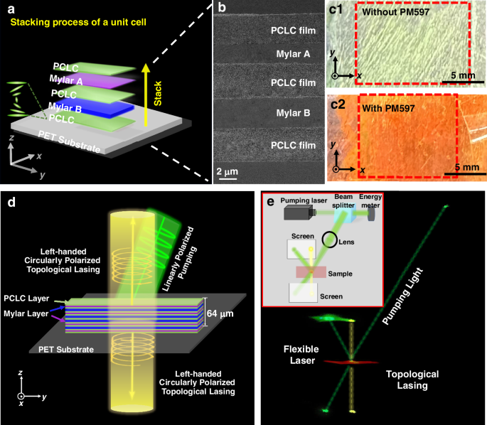
In order to experimentally realize a topological VCSEL, we prepare the soft-matter-based metastructural superlattice cavity by vertically stacking left-handed PCLC films and commercial Mylar films, without any complex lithography or deposition technique. The stacking diagram and the cross-sectional SEM image of one unit cell are shown in Fig. 4a, b. It consists of two Mylar films of different thicknesses (3 μm and 4 μm) and three PCLC films of the same thickness (4 μm). As can be seen from the Fig. 4b, layers are stacked closely and remain flat. By spin-coating a gain medium (Pyrromethene 597 – PM597, solution 1 wt.% in ethanol) with a negligible thickness on each PCLC film, a flexible, free-standing, circularly polarized topological VCSEL can be achieved. Figure 4c1, c2 shows the photographs of two samples with and without PM597, respectively, consisting of 17-layer films on a flexible PET substrate according to the metastructural superlattice shown in Fig. 4d, which is also consistent with the theoretical model in Fig. 3a. The areas framed by the red dashed lines are the effective regions. Here, we used a tape to fix the sample on the substrate at its edges for the purpose of experimental testing. In fact, one can use highly transparent double-faced adhesive tape to attach the film sample virtually to any substrate.
a Schematic diagram of one unit cell with five stacked layers. b Cross-sectional SEM image of one unit cell of the topological VCSEL. c Pictures of the optical superlattices consisting of 17 layers without (c1) and with (c2) the dye PM597. The areas marked by the red dashed lines are the effective regions of the samples. d Illustration diagram of dual-side lasing when pumped by linearly polarized light. The thin film is parallel to the x-y plane, and lasing emissions are along the z and –z directions. e A photograph of actual output lasing patterns from two sides of the sample. Due to the fluorescent dye PM597, the film appears purplish red. Two yellow light spots at the direction perpendicular to the sample represent the left-handed circularly polarized TIS laser emission, while the green light spots represent the pump light. The inset shows the corresponding experimental setup
In the experiments, we use a frequency-doubled \({\rm{Q}}\)-switched Nd:YAG laser (SLIII-10, Continuum) with an output wavelength of 532 nm, a repetition rate at 10.0 Hz, and a pulse duration of 4.0 ns to excite the sample. Left-handed circularly polarized topological lasing at 575.4 nm is observed from this soft-matter-based topological VCSEL, as shown in Fig. 4d, where two yellow laser beams are illustrated in opposite directions perpendicular to the surface. This wavelength is consistent with that of the TIS in the transmission spectrum calculated theoretically and experimentally (Fig. 3c and Supplementary Fig. S4). A photograph of the actual lasing beam output is shown in Fig. 4e, where the inset shows the specific experimental setup. From this photograph, one can see the lasing and pump light spots on the screens, mirror and sample due to scattering. In order to clearly show the paths of the pump beam and the topological lasing beam, dotted lines are added in Fig. 4e.
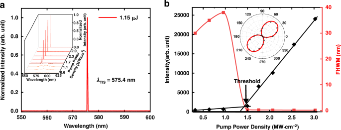
We further examine the topological lasing threshold and polarization characteristics through the experimental setup as described in Materials and Methods. In order to improve the spectral characterization and eliminate influence from fluorescent background, we placed the objective lens 2.0 cm behind the sample. Figure 5a shows the single-mode TIS lasing with a peak wavelength of 575.4 nm at a pump energy of 1.15 μJ, and the inset shows the emission spectra under different pump power densities. From Fig. 5b, it can be found that when the pumping energy exceeds 0.47 μJ (1.5 MW∙cm−2), the full width at half maximum (FWHM) of the emission peak is obviously narrowed and finally reaches 0.13 nm, indicating the lasing behavior. We also measured the beam divergence angle of the laser by using a beam profile analyzer testing the intensity distribution of laser spots. According to the measurements shown in the Supplementary Note 6 of the SI, the divergence angle of the lasing beam decreases to 3° after the threshold, confirming that our topological VCSEL achieves directional emission. In addition, as the pump energy is larger than 4.4 μJ, other defect states in the superlattice will also be excited. Our experimental results show that the threshold of the TIS lasing is significantly lower than that required to excite those other defect states, because the TIS in the superlattice has the highest photonic density of state. In addition, we also conducted theoretical simulations of our topological VCSEL (see Supplementary Note 7 of the SI). The wavelength of the topological lasing obtained in the calculated emission spectrum has a good correspondence with the experimental result. Meanwhile, the calculated spatial distribution shows that TIS is mainly localized at the interface, which is also in good agreement with the results calculated through the tight-binding model (Figs. 2b and 3b). A quartz quarter-wave plate with its slow axis parallel to the vertical axis and a polarizer are used to examine the polarization characteristics of the TIS lasing. As shown in the inset of Fig. 5b, when the polarizer is rotated to 45° and 225° relative to the horizontal axis, the transmitted intensity is maximum, while the lasing is completely wiped out at 135° and 315°, indicating that the TIS lasing emitted from the topological VCSEL has a good left-handed circular polarization characteristic. Besides, its lasing slope efficiency reaches 4.0%, and its total lasing conversion efficiency (the ratio of lasing pulse energy to pump pulse energy) reaches 3.8% under the pump energy of 2.0 μJ.
a Emission spectrum obtained from the superlattice pumped at 1.15 μJ. The inset shows the emission spectra at different pump energies. b Plot of the peak intensity and FWHM of the TIS emission as a function of the pump power density. The laser threshold indicated by an arrow in the figure is 1.5 MW∙cm−2. The inset shows the intensity of the quarter-waveplate-transformed laser radiation as a function of the polarization angle in polar coordinates. The polar angle stands for the transmission angle of the polarizer, and the radius stands for the transmittance
Two application examples of the flexible topological VCSEL
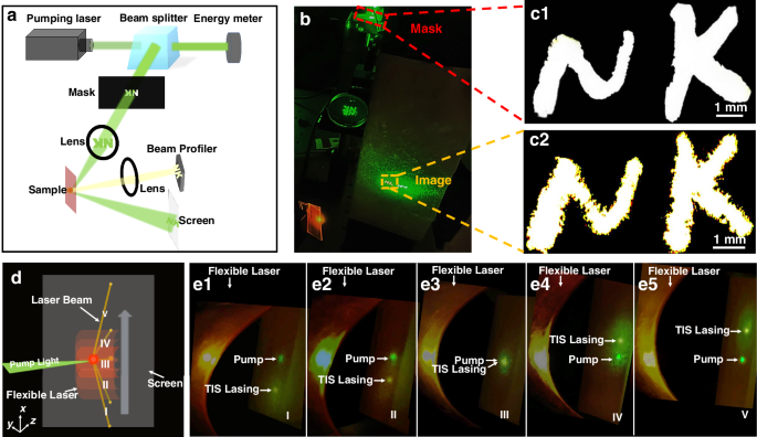
Our topological VCSEL not only maintains good single longitudinal mode emission under low pump intensity, but it also carries the spatial information of the pump light, i.e., its spatial profile is determined by the pump light. To illustrate this, a photomask engraved with two letters ‘NK’ is inserted into the pump light path and imaged on the sample by a lens with a focal length of 85 mm. The topological lasing pattern is monitored by a laser beam profiler (SP620U, Ophir-Spiricon) through another lens, as shown in Fig. 6a. As illustrated in Fig. 6b, the pump beam reflected by the sample and the lasing beam can both be displayed on a screen. Figure 6c2 clearly shows the transverse profile of the topological laser, which corresponds well to the photomask shown in Fig. 6c1. Therefore, our topological VCSEL has a great potential to be used in optical display devices. Compared with the traditional optical display devices, it exhibits excellent circular polarization properties, which offers enhanced contrast and improved viewing comfort – features particularly appealing for 3D displays. Importantly, since the helical axis of the PCLC remains perpendicular to the film surface, lasing performance can be maintained during bending. However, there exist several limitations too. For instance, the lasing wavelength cannot be flexibly tuned as in other liquid crystal display devices, the fidelity of far-field images and the laser conversion efficiency are still relatively low, requiring further optimization to meet the demands for practical applications.
a Experimental setup and b photograph demonstrating a topological VCSEL excited by a pump beam passing through a photomask containing the letters ‘NK’. c Photographs of the photomask (c1) and the topological lasing pattern (c2). The black area of the mask is opaque, while the white area of ‘NK’ is transparent. d Illustration diagram of the laser beam steering caused by shifting the curved VCSEL sample. e1–5 Experimental photographs taken when the sample is moved upward, and thus the laser illuminates at different positions on the screen (I–V)
Finally, to demonstrate the flexibility of the topological VCSEL, we design an experiment in which the laser beam can be diverted and redirected by moving a curved VCSEL film (see Fig. 1a). As illustrated in Fig. 6d, the sample is bent into a cylindrical surface by fixing it on a cylinder, and moved from bottom to top. As a result, the pump beam of the Nd:YAG laser illuminates different regions of the cylindrical film, so that five different locations on the film are pumped subsequently, labeled as I-V. The deformation of the film causes the helical axes of the PCLCs along different normal directions of the cylindrical surface, which in turn moves the outgoing lasing spots to fall on the screen at different locations. As shown in Fig. 6e1–5, the corresponding TIS lasing spots (yellow spots) and pump lasing spots (green spots) can be seen on the screen, showing the beam steering phenomenon with the flexible topological VCSEL. Adjusting the radius of curvature of the VCSEL film can further control the beam steering degree. This property means that the topological VCSEL can lase in a range of directions without rotating the laser device. Notably, the topological VCSEL is thermally stable and retains its original lasing characteristics once re-pumped even after a long period of time, as shown in the Supplementary Note 8 of the SI. These characteristics of the laser device are particularly attractive for potential wearable photonic technologies and compatible platforms.

