

Scientists have built tiny “light racetracks” that could supercharge the next generation of sensors and photonic devices.
Researchers at the University of Colorado at Boulder have developed high-performance optical microresonators that could help power a new generation of advanced sensors.
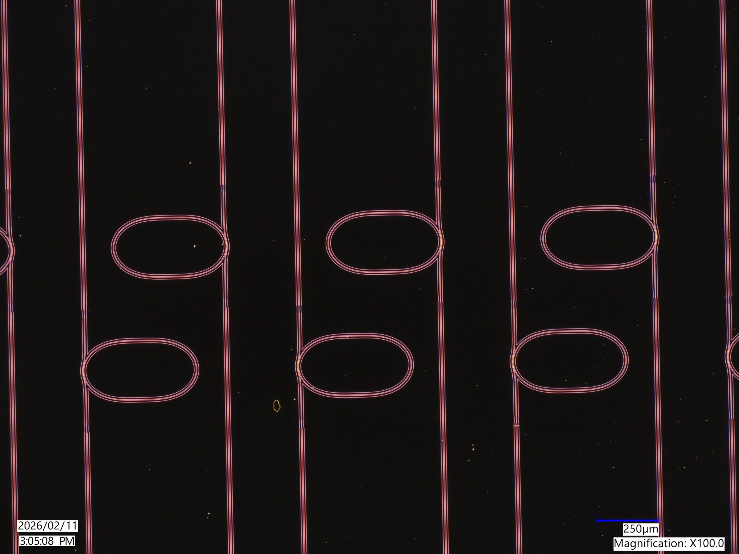
A microresonator is a tiny structure designed to confine light in a very small space. As light circulates inside, its intensity builds. When that intensity reaches a high enough level, scientists can trigger specialized optical effects that make the device useful for sensing and other applications.
“Our work is about using less optical power with these resonators for future uses,” said Bright Lu, a fourth year doctoral student in electrical and computer engineering and a lead author of the study. “One day these microresonators can be adapted for a wide range of sensors from navigation to identifying chemicals.”
The findings were published today (February 23) in Applied Physics Letters.
Racetrack Design Reduces Light Loss
The team concentrated on so-called “racetrack” resonators, named for their elongated loop shape that resembles a running track.
To improve performance, they incorporated “Euler curves”—a type of smooth curve also found in the design of roads and railways. Just as vehicles cannot handle sudden right-angle turns at speed, light does not travel efficiently through sharp corners.
“These racetrack curves minimize bending loss,” said Won Park, Sheppard Professor of Electrical Engineering and co-advisor on the study. “Our design choice was a key innovation of this project.”
By guiding light along gradual, carefully engineered curves, the researchers significantly reduced the amount of light that escapes. This allows photons to circle inside the device longer and interact more strongly.
Lu explained that if too much light leaks out, the device cannot reach the high intensities required for top performance.
Built in a Precision Clean Room
The microresonators are incredibly small and were fabricated at the Colorado Shared Instrumentation in Nanofabrication and Characterization (COSINC) clean room using a new electron beam lithography system.
Such facilities provide tightly controlled environments that are essential when working at microscopic scales. Many photonic components are smaller than the thickness of a sheet of paper, so even tiny dust particles or surface flaws can interfere with how light moves through them.
“Traditional lithography uses photons and is fundamentally limited by the wavelength of light,” Lu said. “However, electron beam lithography has no such constraint. With electrons, we can realize our structures with sub-nanometer resolution, which is critical for our microresonators.”
Lu said the fabrication process was one of the most rewarding parts of the project.
“Clean rooms are just cool. You’re working with these massive, precise machines, and then you get to see images of structures you made only microns wide. Turning a thin film of glass into a working optical circuit is really satisfying.”
Chalcogenide Glass Boosts Performance
A major achievement of the project was successfully building the devices from chalcogenides, a group of specialized semiconductor glasses.
“These chalcogenides are excellent materials for photonics because of their high transparency and nonlinearity,” Park said. “Our work represents one of the best-performing devices using chalcogenides, if not the best.”
Chalcogenides are especially useful because they allow intense light to pass through with minimal loss, which is essential for microresonators. At the same time, they are challenging materials to process, requiring careful optimization.
“Chalcogenides are difficult, but rewarding materials to operate for photonic nonlinear devices,” said Professor Juilet Gopinath, who has collaborated with Park on this effort for more than 10 years. “Our results showed that minimizing the bend loss enables ultra-low loss devices comparable to state-of-the-art in other materials platforms.”
Measuring Light at the Microscale
After fabrication, the devices were tested under the direction of James Erikson, a physics PhD student who specializes in laser based measurements. He precisely aligned lasers with microscopic waveguides, sending light into and out of the resonators while tracking its behavior inside.
The team searched for small “dips” in the transmitted light signal that reveal when photons are resonating within the structure. By examining the shape of those dips, they determined characteristics such as absorption and heating effects.
“The most obvious indicator of device quality is the shape of the resonances, and we want them to be deep and narrow, like a needle piercing through the signal background,” Erikson said. “We’ve been chasing this kind of resonator for a long time, and when we saw the sharp resonances on this new devic,e we knew right away that we’d finally cracked the code.”
He added that understanding how much light is absorbed versus transmitted is critical. As laser power increases, heating can become a concern and may even damage the device.
“The way most materials interact with light also changes depending on the temperature of the material,” said Erikson. “So as a device heats up its properties can change and cause it to work differently.”
Toward Microlasers and Quantum Technologies
Looking ahead, the researchers believe these microresonators could enable compact microlasers, highly sensitive chemical and biological detectors, and tools for quantum metrology and networking.
“Many photonic components from lasers, modulators, and detectors are being developed, and microresonators like ours will help tie all of those pieces together,” Lu said. “Eventually, the goal is to build something you could hand to a manufacturer and create hundreds of thousands of them.”
Reference: 23 February 2026, Applied Physics Letters.
DOI: 10.1063/5.0305459
Never miss a breakthrough: Join the SciTechDaily newsletter.
Follow us on Google and Google News.